Semiconductor and ElectronicsReport ID: MR-2143Aug 2026320 PagesGlobal
Verified by the Meticulous Standard·Last verified: May 2026 by Specialist Analyst

Semiconductor Ultrapure Water Systems Market by System Component (Pretreatment, Primary Purification, Advanced Polishing), Technology, UPW Quality Requirement, Application, Fab Type, End User, and Geography - Global Forecast to 2036

Published Date: Aug 2026
Format: PDF + Excel + Cloud Portal
Pages / Size: 320 Pages
Analyst: Specialist Analyst
Secure checkout · Full methodology disclosure · Underwritten by lead analyst Specialist Analyst
Semiconductor Ultrapure Water Systems Market Size
Semiconductor Ultrapure Water Systems Market Sizing & Sourcing
Base year: 2025 · CAGR: 7.2%
$5.86B
Market size 2025
$6.42B
Market size 2026
$12.84B
Forecast by 2036
7.2%
CAGR 2026–2036

Market Overview

Semiconductor Ultrapure Water Systems Market Size

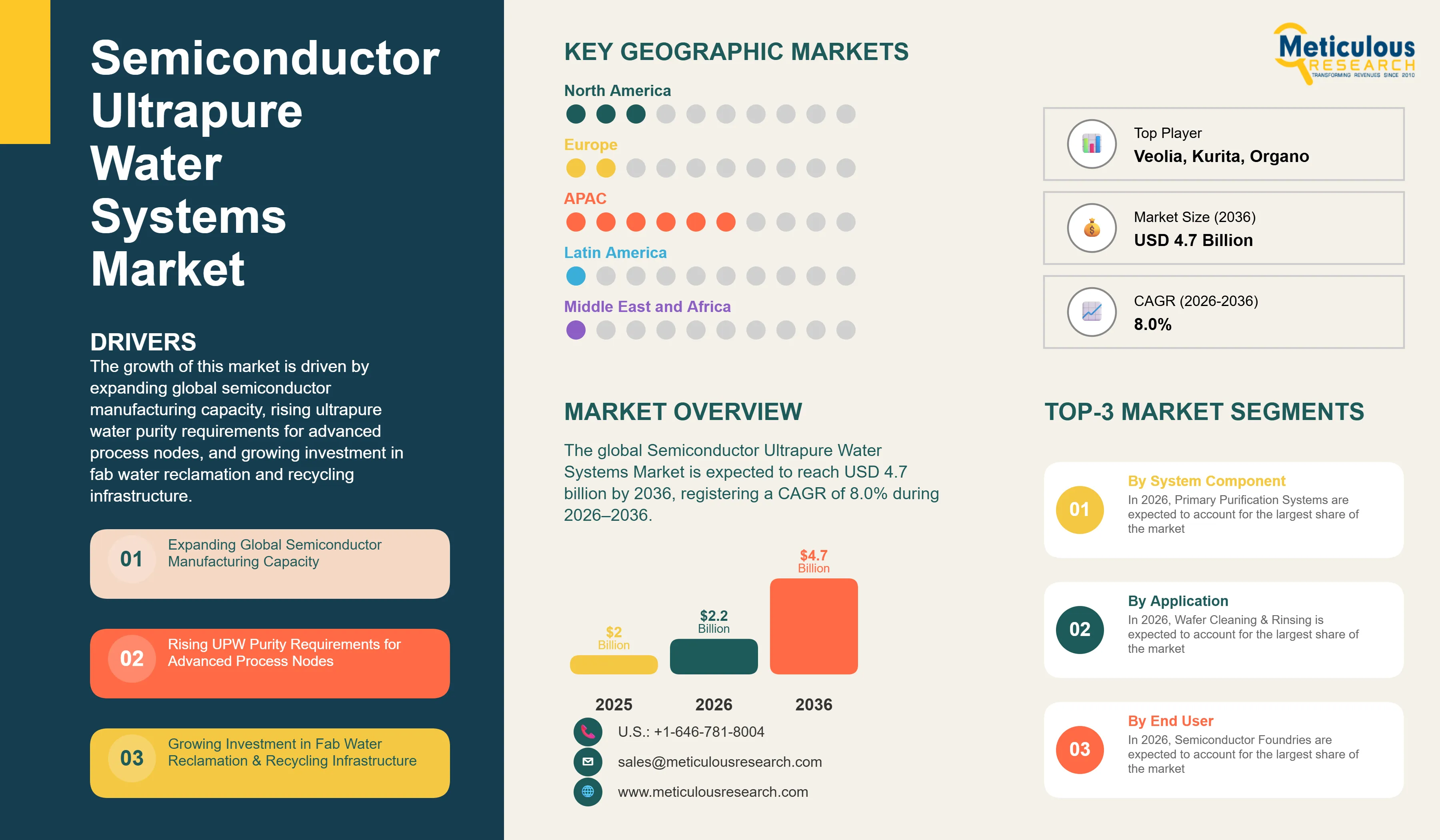
The global Semiconductor Ultrapure Water Systems Market was valued at USD 2.0 billion in 2025 and is projected to reach USD 2.2 billion in 2026. The market is expected to reach USD 4.7 billion by 2036, registering a CAGR of 8.0% during the forecast period (2026–2036).

Key Highlights

  • The global Semiconductor Ultrapure Water Systems Market is projected to reach USD 4.7 billion by 2036, driven by expanding global semiconductor manufacturing capacity, rising UPW purity requirements for advanced process nodes, and growing investment in fab water reclamation and recycling infrastructure.
  • Asia-Pacific is expected to account for the largest market share in 2026, while North America is projected to register the fastest growth during the forecast period.
  • By system component, Primary Purification Systems are expected to account for the largest market share, whereas UPW Reclamation & Recycling Systems are projected to witness the fastest growth through 2036.
  • By technology, Reverse Osmosis is expected to remain the dominant purification technology, while Advanced Oxidation Processes are projected to register the highest CAGR as fabs seek tighter contaminant control.
  • A typical semiconductor fabrication facility consumes up to 10 million gallons of ultrapure water per day, underscoring the scale and criticality of UPW infrastructure to fab operations.
  • Record global fab equipment spending, projected to reach USD 133 billion in 2026 and exceed USD 150 billion in 2027, is expected to create substantial long-term demand for new UPW system installations.

Executive Summary

The Semiconductor Ultrapure Water Systems Market comprises the equipment, technologies, and services used to treat raw water into ultrapure water meeting the stringent resistivity, total organic carbon (TOC), particle, and metallic contaminant specifications required for semiconductor wafer processing. A complete UPW system spans pretreatment, primary purification (including reverse osmosis, electrodeionization, and ion exchange), advanced polishing (UV oxidation, ultrafiltration, and mixed-bed ion exchange), storage and distribution, monitoring and control, and increasingly, reclamation and recycling systems designed to recover water for reuse within the fab.

Water is one of the largest-volume process inputs in semiconductor manufacturing, and demand for UPW systems is directly tied to the pace of fab construction and capacity expansion. According to the World Economic Forum, semiconductor manufacturing can require millions of gallons of water per day at a single large facility, with water used extensively for wafer cleaning, rinsing, cooling, and other process applications. TSMC, one of the world's largest semiconductor manufacturers, reported that its global water consumption reached approximately 27.3 million cubic meters in 2024, highlighting the enormous water requirements associated with large-scale semiconductor production. This water intensity, combined with the hundreds of cleaning and rinsing steps performed during wafer fabrication, makes ultrapure water systems a mission-critical investment for semiconductor fabs. Increasing water scarcity and regulatory pressure are also encouraging manufacturers to incorporate advanced reclamation, recycling, and closed-loop UPW systems into new and existing facilities.

The market is benefiting from record levels of global semiconductor manufacturing investment. According to SEMI's latest 300mm Fab Outlook, global 300mm fab equipment spending is projected to reach approximately US$142 billion in 2026, representing a 25% increase from 2025. SEMI also forecasts global 300mm fab equipment spending to reach approximately US$156 billion in 2027, as AI, high-performance computing, advanced logic, and memory demand drive continued capacity expansion. SEMI is tracking more than 1,500 fabs and production lines worldwide, with substantial new capacity being added across Asia-Pacific, North America, and Europe. As UPW systems represent a foundational element of fab facility infrastructure, this sustained wave of capacity expansion is directly translating into rising demand for new UPW system installations, capacity expansions, water-reclamation systems, advanced polishing equipment, and monitoring technologies.

Market Growth Drivers

Expansion of Global Semiconductor Manufacturing Capacity

Sustained global investment in semiconductor manufacturing capacity, with SEMI projecting worldwide 300mm fab equipment spending to reach USD 133 billion in 2026 and USD 151 billion in 2027, is directly driving demand for new UPW systems, as every new fab requires a complete, purpose-built ultrapure water infrastructure before wafer production can begin.

Increasing Construction of Advanced Semiconductor Fabs

Major semiconductor manufacturers are constructing new fabs across the United States, Taiwan, South Korea, Japan, and Europe to support both leading-edge and mature-node production, supported by regional policy incentives aimed at strengthening semiconductor supply chain resilience. Each new fab construction project requires large-scale UPW system design, engineering, and installation, creating a direct and sustained revenue opportunity for UPW system suppliers.

Market Restraints

High Capital Investment Requirements

A complete semiconductor-grade UPW system, encompassing pretreatment, multi-stage purification, polishing, and distribution infrastructure, requires substantial upfront capital investment. This high capital intensity can be a barrier for smaller fabs and facilities in emerging semiconductor manufacturing locations with more constrained capital budgets.

High Energy and Operating Costs

UPW production is highly energy-intensive, with filtration and reverse osmosis processes reported to account for over 60% of operational energy usage in typical semiconductor fabs. These elevated ongoing energy and operating costs represent a significant lifecycle cost consideration for fab operators evaluating UPW system investments.

Market Opportunities

Expansion of AI, HPC, and Advanced Semiconductor Manufacturing

The rapid growth of AI accelerator and high-performance computing chip demand is driving substantial new fab investment, with SEMI citing AI-fueled demand as a primary factor resetting the scale of global semiconductor manufacturing investment. This expansion is creating sustained opportunities for UPW system suppliers serving new leading-edge fab construction projects.

Increasing Adoption of UPW Recycling and Reclamation

Water scarcity concerns and sustainability commitments are driving fabs to invest in water reclamation and near-zero liquid discharge systems. Leading manufacturers such as TSMC have targeted water recycling rates exceeding 90% at select facilities, creating a substantial and growing opportunity for suppliers of membrane-based, RO-based, and advanced oxidation-based UPW reclamation technologies.

Market Challenges

Increasing Difficulty of Removing Trace Contaminants

As process nodes shrink below 3nm, even trace-level ionic, organic, and particulate contaminants that were previously acceptable can now cause yield-damaging defects. Achieving and consistently maintaining these increasingly stringent purity thresholds presents an ongoing technical challenge for UPW system designers and operators.

Management of Nanometer-Scale Particles

Advanced-node wafer processing requires UPW systems capable of reliably removing particles at the nanometer scale, a level of filtration precision that pushes the limits of current ultrafiltration and sub-micron filtration technologies and requires continuous technology investment to keep pace with shrinking device geometries.

Market Trends

Growing Adoption of Zero-Liquid-Discharge and Water Reclamation Systems

Leading semiconductor manufacturers are increasingly investing in near-zero liquid discharge infrastructure to recycle industrial wastewater back into UPW-grade water. TSMC, for example, has targeted recycling 90% or more of total water consumption at select facilities, reflecting a broader industry trend toward closed-loop water management as a core element of fab sustainability strategy.

Rising Integration of Digital UPW Monitoring and Predictive Maintenance

Fabs are increasingly deploying real-time digital monitoring systems for resistivity, TOC, particle counts, and dissolved oxygen, combined with predictive maintenance analytics, to reduce the risk of UPW quality excursions that can damage wafer yield. This shift toward digitalized, condition-based UPW system management is expected to play a growing role in reducing unplanned production disruptions.

Segment Analysis

Market Analysis by System Component

Based on system component, the global Semiconductor Ultrapure Water Systems Market is segmented into Pretreatment Systems, Primary Purification Systems, Advanced Polishing Systems, UPW Storage & Distribution Systems, UPW Monitoring & Control Systems, UPW Reclamation & Recycling Systems, and Services.

In 2026, Primary Purification Systems are expected to account for the largest market share, reflecting the central role of reverse osmosis, electrodeionization, and ion exchange technologies in achieving baseline UPW quality. However, UPW Reclamation & Recycling Systems are projected to register the fastest growth during the forecast period, driven by growing fab investment in water recycling and near-zero liquid discharge infrastructure amid rising water scarcity concerns.

Market Analysis by Technology

Based on technology, the market is segmented into Reverse Osmosis, Ion Exchange, Electrodeionization, Ultrafiltration, Microfiltration, UV Oxidation, Membrane Degasification, Ozone Treatment, Advanced Oxidation, and Other Technologies.

In 2026, Reverse Osmosis is expected to account for the largest market share, owing to its established role as the primary purification technology across nearly all semiconductor UPW systems. However, Advanced Oxidation Processes are projected to register the highest CAGR, as fabs increasingly adopt these technologies to achieve tighter TOC and trace organic contaminant control required for advanced process nodes.

Market Analysis by UPW Quality Requirement

Based on UPW quality requirement, the market is segmented into Standard Semiconductor-Grade UPW, Advanced-Node UPW, Ultra-Low TOC UPW, Ultra-Low Metal UPW, Ultra-Low Particle UPW, and Hot Ultrapure Water (HUPW).

In 2026, Standard Semiconductor-Grade UPW is expected to account for the largest market share, reflecting its continued use across mature-node and legacy fab production. However, Advanced-Node UPW is projected to register the highest CAGR, driven by the ongoing global transition toward sub-3nm process technologies and EUV lithography that demand progressively tighter purity specifications.

Market Analysis by Application

Based on application, the market is segmented into Wafer Cleaning & Rinsing, Photolithography, Etching, Chemical Mechanical Planarization, Deposition & Thin-Film Processing, Wafer Dicing & Back-End Processing, and Advanced Packaging.

In 2026, Wafer Cleaning & Rinsing is expected to account for the largest market share, given that each wafer undergoes hundreds of UPW-intensive cleaning and rinsing steps throughout the fabrication process. However, Advanced Packaging is projected to register the highest CAGR, driven by rapid growth in 2.5D, 3D, and hybrid bonding packaging technologies supporting AI and high-performance computing chip demand.

Market Analysis by Fab Type

Based on fab type, the market is segmented into Logic & Foundry Fabs, Memory Fabs (DRAM, NAND, and HBM), Analog & Power Semiconductor Fabs, Compound Semiconductor Fabs (Silicon Carbide and Gallium Nitride), MEMS & Sensor Fabs, and Advanced Packaging Facilities.

In 2026, Logic & Foundry Fabs are expected to account for the largest market share, consistent with SEMI's data identifying Logic & Micro, including Foundry, as the largest segment of global fab equipment spending. However, HBM Manufacturing Fabs, within the Memory Fabs segment, are projected to register the fastest growth, supported by surging demand for high-bandwidth memory used in AI accelerator chips.

Market Analysis by End User

Based on end user, the market is segmented into Semiconductor Foundries, Integrated Device Manufacturers (IDMs), Memory Manufacturers, Compound Semiconductor Manufacturers, MEMS & Sensor Manufacturers, Advanced Packaging & OSAT Providers, and Semiconductor Research & Development Facilities.

In 2026, Semiconductor Foundries are expected to account for the largest market share, reflecting the scale of new fab construction underway among leading contract manufacturers. However, Advanced Packaging & OSAT Providers are projected to register the highest CAGR, driven by rising UPW requirements for advanced packaging processes supporting next-generation chip architectures.
Geographical Analysis

Based on geography, the global Semiconductor Ultrapure Water Systems Market is segmented into North America, Europe, Asia-Pacific, Latin America, and the Middle East & Africa.

In 2026, Asia-Pacific is expected to account for the largest share of the global Semiconductor Ultrapure Water Systems Market. The region's leadership is supported by the concentration of the world's largest semiconductor manufacturing capacity in Taiwan, South Korea, China, and Japan. According to SEMI, China, Taiwan, and Korea are expected to remain the top three destinations for global semiconductor equipment spending, with Taiwan's leading-edge foundry capacity expansion, including 2nm and sub-2nm technologies, requiring substantial new UPW system investment to support production ramp-up.

However, North America is projected to register the highest CAGR during the forecast period. The region's growth is driven by large-scale new fab construction supported by domestic semiconductor manufacturing incentives, with SEMI projecting the Americas to invest approximately USD 60 billion in 300mm fab equipment between 2026 and 2028. Individual projects such as TSMC's Arizona campus, which has grown to a planned USD 165 billion total investment across multiple fabs, require dedicated UPW infrastructure capable of supporting up to 14 million gallons per day of water withdrawal at full build-out, directly driving regional demand for new UPW system installations and water reclamation infrastructure.

Competitive Landscape

The global Semiconductor Ultrapure Water Systems Market is moderately consolidated, with competition among large, diversified water technology companies, specialized semiconductor water treatment providers, and component-level suppliers of membranes, resins, and monitoring instrumentation. Companies compete primarily on system reliability, purity performance consistency, engineering and integration expertise, global service network coverage, and increasingly, water recycling and sustainability credentials.

Leading market participants are investing in expanding UPW reclamation and zero-liquid-discharge system capabilities, developing digital monitoring and predictive maintenance platforms, and forming strategic partnerships with leading semiconductor manufacturers to secure long-term system supply and service agreements tied to major new fab construction projects. Capacity expansions, technology upgrades, and water sustainability-focused product development remain key strategies adopted by major vendors.

The report provides a comprehensive competitive assessment of the leading companies operating in the global Semiconductor Ultrapure Water Systems Market. The key players profiled in the report include Veolia Water Technologies, SUEZ Water Technologies & Solutions, Xylem Inc., Kurita Water Industries Ltd., Organo Corporation, DuPont de Nemours, Inc., Pentair plc, Ovivo Inc., Aquatech International LLC, MIOX Corporation, A.O. Smith Corporation, Asahi Kasei Corporation, Toray Industries, Inc., Mitsubishi Chemical Group Corporation, and Pall Corporation.

Market Research Summary

Particulars

Details

Forecast Period

2026–2036

Base Year

2025

Estimated Year

2026

CAGR (Value)

8.0%

Market Size (Value) in 2026

USD 2.2 Billion

Market Size (Value) in 2036

USD 4.7 Billion

Segments Covered

By System Component: Pretreatment Systems, Primary Purification Systems, Advanced Polishing Systems, UPW Storage & Distribution Systems, UPW Monitoring & Control Systems, UPW Reclamation & Recycling Systems, Services.

By Treatment Stage: Pretreatment, Makeup Water Treatment, Primary Purification, Polishing, Point-of-Use Treatment, UPW Distribution, UPW Reclamation & Recycling.

By Technology: Reverse Osmosis, Ion Exchange, Electrodeionization, Ultrafiltration, Microfiltration, UV Oxidation, Membrane Degasification, Ozone Treatment, Advanced Oxidation, Other Technologies.

By UPW Quality Requirement: Standard Semiconductor-Grade UPW, Advanced-Node UPW, Ultra-Low TOC UPW, Ultra-Low Metal UPW, Ultra-Low Particle UPW, Hot Ultrapure Water (HUPW).

By Application: Wafer Cleaning & Rinsing, Photolithography, Etching, Chemical Mechanical Planarization, Deposition & Thin-Film Processing, Wafer Dicing & Back-End Processing, Advanced Packaging.

By Fab Type: Logic & Foundry Fabs, Memory Fabs (DRAM, NAND, HBM), Analog & Power Semiconductor Fabs, Compound Semiconductor Fabs (SiC, GaN), MEMS & Sensor Fabs, Advanced Packaging Facilities.

By Fab Size: Small-Scale Fabs, Medium-Scale Fabs, Large-Scale Fabs, Mega Fabs.

By End User: Semiconductor Foundries, Integrated Device Manufacturers (IDMs), Memory Manufacturers, Compound Semiconductor Manufacturers, MEMS & Sensor Manufacturers, Advanced Packaging & OSAT Providers, Semiconductor R&D Facilities.

Countries Covered

North America: U.S., Canada.

Europe: Germany, France, U.K., Netherlands, Belgium, Ireland, Italy, Rest of Europe.

Asia-Pacific: Taiwan, China, South Korea, Japan, Singapore, India, Malaysia, Vietnam, Rest of Asia-Pacific.

Latin America: Brazil, Mexico, Argentina, Rest of Latin America.

Middle East & Africa: Israel, UAE, Saudi Arabia, South Africa, Rest of Middle East & Africa.

Key Companies

Veolia Water Technologies, SUEZ Water Technologies & Solutions, Xylem Inc., Kurita Water Industries Ltd., Organo Corporation, DuPont de Nemours, Inc., Pentair plc, Ovivo Inc., Aquatech International LLC, MIOX Corporation, A.O. Smith Corporation, Asahi Kasei Corporation, Toray Industries, Inc., Mitsubishi Chemical Group Corporation, and Pall Corporation.

Key Questions Answered

Frequently Asked Questions

How We Built This Intelligence

Table of Contents

Expand all

Access & Licensing

Choose how you access this intelligence — from a standalone data pack to organization-wide access. Every option is delivered within 24–48 hours and backed by analyst support.

Single User License
Instant access to full PDF report + Excel dataset.
$4,175
1–5 User Access
Full PDF Report + Excel Datasheets
1-Hour Analyst Call included
Free 10% Customization
POPULAR
Multi-User License
Instant access to full PDF report + Excel dataset.
$5,875
1–5 User Access
Full PDF Report + Excel Datasheets
1-Hour Analyst Call included
Free 10% Customization
Enterprise License
Instant access to full PDF report + Excel dataset.
$7,875
1–5 User Access
Full PDF Report + Excel Datasheets
1-Hour Analyst Call included
Free 10% Customization
Flexible Purchase Options
Buy the complete report, individual chapters, or only the data you need. Starting from $1,500.
Analyst-reviewed intelligence
Multi-source validation
Transparent methodology
Citation-ready data
Analyst assistance

Related Statistics & Insights

$2.0B
market value in 2025
$4.7B
projected market value by 2036
8.0%
compound annual growth rate
$156billion
in 2027, as AI, high-performance computing, advanced logic, and memory demand drive continued…
Cite this report
Meticulous Research. (2026). Semiconductor Ultrapure Water Systems Market - Global Opportunity Analysis and Industry Forecast to 2036 (Report No. MR-2143). Meticulous Market Research Pvt. Ltd. https://meticulousresearch.com/reports/semiconductor-ultrapure-water-systems-market-6826
Custom Research

Need something more specific?

A custom-scoped study can target a single segment, geography, or competitor set — or answer a board-level question this syndicated report doesn't. Tell an analyst what decision you're making and we'll scope it.

Search Market Intelligence

Search across reports, blogs, press releases, and industries