Semiconductor and ElectronicsReport ID: MR-2147Aug 2026288 PagesGlobal
Verified by the Meticulous Standard·Last verified: May 2026 by Specialist Analyst

HBM Inspection Equipment Market by Equipment Type (Optical, 3D Optical Metrology, X-Ray, Infrared), Inspection Technique, Inspection Stage, HBM Generation, Stack Height, Stacking & Bonding Technology, End User, and Geography - Global Forecast to 2036

Published Date: Aug 2026
Format: PDF + Excel + Cloud Portal
Pages / Size: 288 Pages
Analyst: Specialist Analyst
Secure checkout · Full methodology disclosure · Underwritten by lead analyst Specialist Analyst
HBM Inspection Equipment Market Size
HBM Inspection Equipment Market Sizing & Sourcing
Base year: 2025 · CAGR: 7.2%
$5.86B
Market size 2025
$6.42B
Market size 2026
$12.84B
Forecast by 2036
7.2%
CAGR 2026–2036

Market Overview

HBM Inspection Equipment Market Size

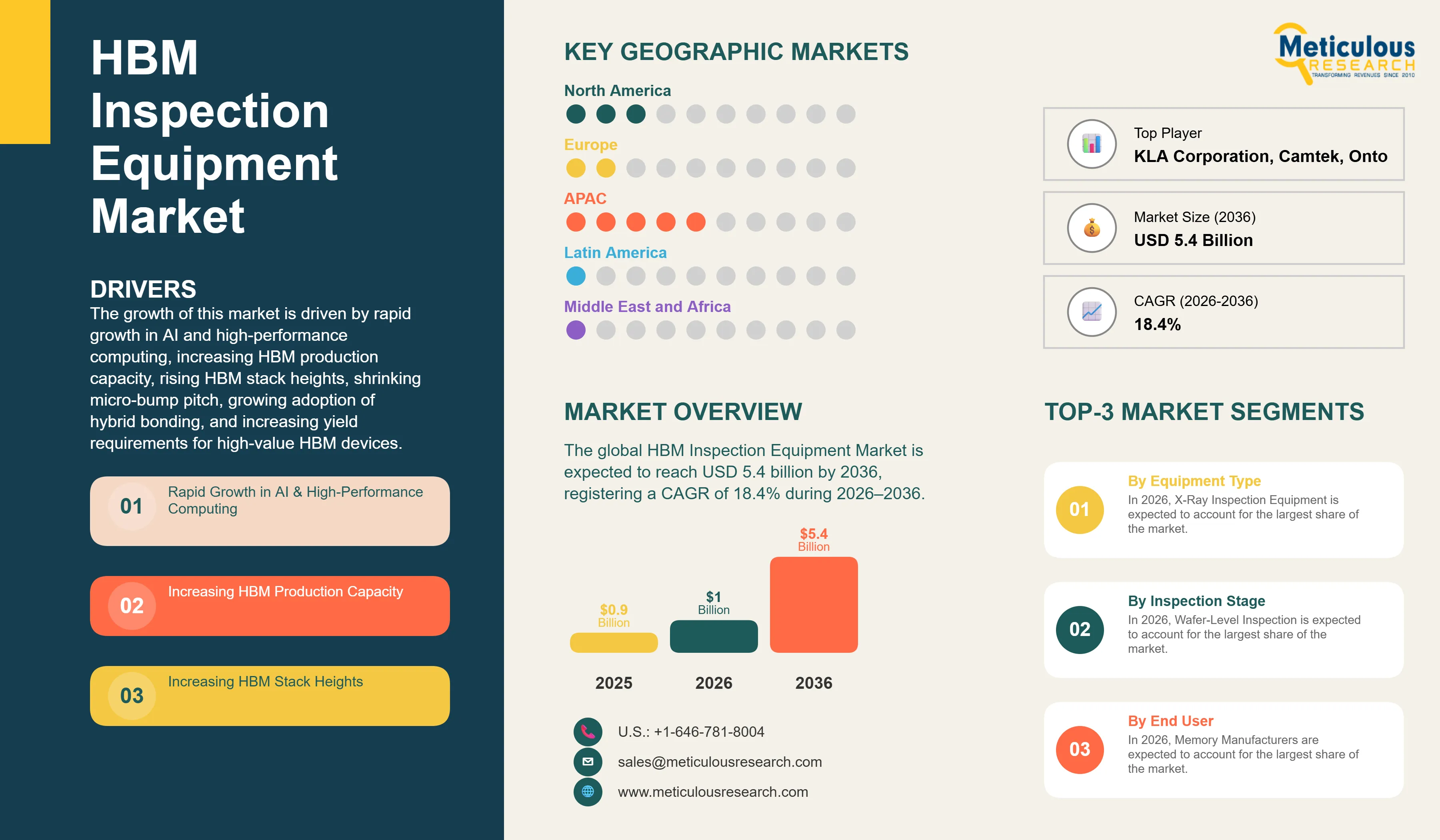
The global HBM Inspection Equipment Market was valued at USD 0.9 billion in 2025 and is projected to reach USD 1.0 billion in 2026. The market is expected to reach USD 5.4 billion by 2036, registering a CAGR of 18.4% during the forecast period (2026–2036).

Key Highlights

  • The global HBM Inspection Equipment Market is projected to reach USD 5.4 billion by 2036, driven by rapid growth in AI and high-performance computing, increasing HBM production capacity, rising stack heights, and shrinking micro-bump pitch across successive HBM generations.
  • Asia-Pacific is expected to account for the largest market share in 2026, while North America is projected to register the fastest growth during the forecast period.
  • By equipment type, X-Ray Inspection Equipment is expected to account for the largest market share, whereas E-Beam Inspection & Metrology Equipment is projected to witness the fastest growth through 2036.
  • The global HBM market is projected to grow from approximately USD 38 billion in 2025 to USD 58 billion in 2026, with industry leaders forecasting sustained annual growth of roughly 30% through 2030, directly driving demand for HBM-specific inspection and metrology capacity.
  • The JEDEC HBM4 standard, released in April 2025, doubles the memory interface to 2,048 bits and enables bandwidth exceeding 2 terabytes per second per stack, introducing more stringent inspection and metrology requirements for next-generation HBM production.
  • Growing adoption of hybrid bonding technology in HBM4 and future HBM generations is expected to create significant long-term opportunities for advanced post-bond and metrology inspection systems.

Executive Summary

The HBM Inspection Equipment Market comprises the specialized inspection, metrology, and defect classification systems used throughout the high-bandwidth memory (HBM) manufacturing process, spanning DRAM wafer inspection, through-silicon via (TSV) inspection, micro-bump and copper pillar metrology, pre-bond and post-bond inspection, internal stack defect detection, and final package-level inspection. HBM production involves stacking multiple DRAM dies vertically using TSVs and micro-bumps or hybrid bonding interconnects, a highly complex three-dimensional packaging process in which even nanometer-scale defects in bump formation, bonding, or die alignment can compromise the electrical performance or yield of the finished memory stack.

Demand for HBM inspection equipment is directly tied to the explosive growth of the HBM market itself, which is being driven by surging demand for AI accelerators, GPUs, and high-performance computing systems. According to industry data, the global HBM market is projected to grow from approximately USD 38 billion in 2025 to USD 58 billion in 2026, with SK Hynix, the market's leading supplier, projecting sustained annual HBM demand growth of roughly 30% through 2030. As HBM producers race to expand capacity and qualify successive generations of increasingly complex stacked memory devices, inspection and metrology equipment has become a critical bottleneck and investment priority across the HBM production line.

The transition to newer HBM generations is significantly increasing inspection complexity and equipment requirements. JEDEC released the official HBM4 specification in April 2025, doubling the memory interface width to 2,048 bits and enabling bandwidth exceeding 2 terabytes per second per stack. HBM4 and subsequent generations are also introducing hybrid bonding and logic base die integration, requiring inspection systems capable of detecting sub-micron bond-line defects, voids, and misalignment across increasingly tall stacks, with leading manufacturers already validating 12-high and 16-high configurations for next-generation AI accelerator platforms.

Market Growth Drivers

Rapid Growth in AI & High-Performance Computing

Surging global demand for AI accelerators, GPUs, and high-performance computing systems is the primary driver of HBM production growth, with the global HBM market projected to expand from approximately USD 38 billion in 2025 to USD 58 billion in 2026. This demand growth translates directly into rising inspection equipment requirements across every stage of the HBM manufacturing and stacking process.

Increasing HBM Production Capacity

Leading memory manufacturers, including SK Hynix, Samsung, and Micron, are aggressively expanding HBM production capacity to meet AI accelerator demand, with SK Hynix projecting approximately 30% annual HBM demand growth through 2030. Each new production line requires a full suite of wafer-level, pre-bond, post-bond, and final inspection equipment, directly driving sustained capital investment in HBM inspection systems.

Market Restraints

High Cost of Advanced Inspection & Metrology Systems

Advanced HBM inspection systems, particularly 3D X-ray computed tomography and e-beam metrology platforms capable of sub-micron resolution and internal stack visibility, require substantial capital investment. This high cost can limit the pace of inspection capacity expansion, particularly for smaller OSAT providers and emerging HBM manufacturers.

Complex Inspection of Buried and Internal Defects

Detecting defects buried within multi-die HBM stacks, such as internal TSV voids or bond-line delamination between lower dies, requires specialized non-destructive techniques such as X-ray CT and scanning acoustic microscopy that involve inherent trade-offs between resolution, penetration depth, and inspection speed.

Market Opportunities

Increasing Demand for 3D X-Ray & CT Inspection

The growing need to detect internal defects within increasingly tall HBM stacks is driving strong demand for 3D X-ray computed tomography systems capable of non-destructively visualizing TSV voids, bond-line defects, and internal misalignment throughout the full height of the stack, presenting a significant opportunity for suppliers of advanced X-ray CT platforms.

Growing Demand for Inline Post-Bond Inspection

As HBM manufacturers seek to catch bonding defects immediately after each die is stacked rather than waiting for final package testing, demand is growing for inline post-bond inspection systems capable of rapidly detecting bond voids, delamination, and die shift without disrupting production throughput.

Market Trends

Growing Adoption of Multimodal and AI-Enhanced Inspection Platforms

HBM manufacturers are increasingly combining multiple inspection modalities, such as optical, X-ray, and acoustic microscopy, within integrated multimodal platforms, paired with AI-based defect classification software, to achieve comprehensive defect coverage across the full range of HBM defect types while managing inspection throughput requirements.

Rising Demand for Inspection Solutions Tailored to Hybrid Bonding

As hybrid bonding becomes the standard interconnect technology for HBM4 and future generations, inspection and metrology equipment suppliers are increasingly developing purpose-built solutions for hybrid bond-line inspection, copper pad metrology, and surface planarity measurement, reflecting the broader industry shift away from conventional micro-bump architectures.

Segment Analysis

Market Analysis by Equipment Type (Primary Segmentation)

Based on equipment type, the global HBM Inspection Equipment Market is segmented into Optical Inspection Equipment, 3D Optical Metrology Equipment, X-Ray Inspection Equipment, Infrared Inspection Equipment, Scanning Acoustic Microscopy Equipment, E-Beam Inspection & Metrology Equipment, Advanced Inspection Technologies, and Inspection Software & Analytics.

In 2026, X-Ray Inspection Equipment is expected to account for the largest market share, owing to its critical role in non-destructively detecting internal TSV voids and bond-line defects buried within multi-die HBM stacks. However, E-Beam Inspection & Metrology Equipment is projected to register the fastest growth during the forecast period, driven by increasing demand for sub-micron critical dimension and overlay metrology as micro-bump pitch continues to shrink.

Market Analysis by Inspection Technique

Based on inspection technique, the market is segmented into Optical Inspection, 3D Optical Inspection, X-Ray/Computed Tomography, Infrared Inspection, Scanning Acoustic Microscopy, E-Beam Inspection, Terahertz Inspection, and Multimodal Inspection.

In 2026, X-Ray/Computed Tomography is expected to account for the largest market share, reflecting its established role as the primary non-destructive technique for internal stack inspection. However, Multimodal Inspection is projected to register the fastest growth, as manufacturers increasingly combine multiple inspection techniques to achieve comprehensive defect coverage across increasingly complex HBM stack architectures.

Market Analysis by Inspection Stage

Based on inspection stage, the market is segmented into Wafer-Level Inspection, Pre-Bond Inspection, Post-Bond Inspection, Post-Stack Inspection, Final HBM Module Inspection, and Failure Analysis & Process Development.

In 2026, Wafer-Level Inspection is expected to account for the largest market share, reflecting its foundational role in detecting TSV and surface defects before dies enter the stacking process. However, Post-Bond Inspection is projected to register the fastest growth, driven by increasing manufacturer emphasis on catching bonding defects immediately after each die is stacked rather than at final testing.

Market Analysis by HBM Generation

Based on HBM generation, the market is segmented into HBM2, HBM2E, HBM3, HBM3E, HBM4, HBM4E, and Future HBM Generations.

In 2026, HBM3E is expected to account for the largest market share, consistent with its position as the dominant HBM generation in current AI accelerator production. However, HBM4 is projected to register the fastest growth, driven by its April 2025 JEDEC standardization, doubled 2,048-bit interface, and the beginning of full-scale supply from leading memory manufacturers in 2026.

Market Analysis by Stacking & Bonding Technology

Based on stacking and bonding technology, the market is segmented into Thermocompression Bonding, Micro-Bump-Based Stacking, Hybrid Bonding, Die-to-Wafer Stacking, Wafer-to-Wafer Stacking, and Die-to-Die Stacking.

In 2026, Micro-Bump-Based Stacking is expected to account for the largest market share, reflecting its continued use across current-generation HBM3E production. However, Hybrid Bonding is projected to register the fastest growth, driven by its adoption for HBM4 and future generations by leading manufacturers seeking higher interconnect density and improved thermal performance.

Market Analysis by End User

Based on end user, the market is segmented into Memory Manufacturers, Semiconductor Foundries, OSAT Providers, Advanced Packaging Providers, Semiconductor Test Houses, and Research & Development Organizations.

In 2026, Memory Manufacturers are expected to account for the largest market share, reflecting the concentration of HBM production among the three leading global suppliers. However, OSAT Providers are projected to register the fastest growth, driven by increasing outsourcing of advanced HBM packaging and inspection processes as production volumes scale.
Geographical Analysis

Based on geography, the global HBM Inspection Equipment Market is segmented into North America, Europe, Asia-Pacific, Latin America, and the Middle East & Africa.

In 2026, Asia-Pacific is expected to account for the largest share of the global HBM Inspection Equipment Market. The region's leadership is underpinned by the concentration of global HBM production capacity in South Korea and Taiwan, home to SK Hynix and Samsung, which together accounted for the substantial majority of global HBM market share in recent quarters. South Korea's continued investment in HBM4 production ramp-up, alongside Taiwan's advanced packaging ecosystem supporting HBM integration with leading AI accelerator platforms, is driving sustained regional demand for HBM inspection and metrology equipment.

However, North America is projected to register the highest CAGR during the forecast period. The region's growth is driven by Micron's expanding U.S. HBM production capacity and qualification progress with leading AI accelerator customers, alongside strong demand from North American AI accelerator and GPU designers whose qualification and reliability requirements are driving investment in advanced inspection and failure analysis capabilities across the region's semiconductor ecosystem.

Competitive Landscape

The global HBM Inspection Equipment Market is moderately consolidated, with competition among established semiconductor inspection and metrology equipment leaders, specialized advanced packaging inspection providers, and imaging technology companies. Companies compete primarily on defect detection sensitivity, inspection throughput, non-destructive internal inspection capability, AI-based defect classification accuracy, and integration compatibility with HBM production lines.

Leading market participants are investing in developing next-generation X-ray CT and e-beam metrology systems optimized for taller HBM stacks and hybrid bonding architectures, expanding AI-based defect classification software capabilities, and forming strategic partnerships with leading memory manufacturers to co-develop inspection solutions aligned with HBM4 and future generation roadmaps. Capacity expansions, new product launches, and technology partnerships remain key strategies adopted by major vendors.

The report provides a comprehensive competitive assessment of the leading companies operating in the global HBM Inspection Equipment Market. The key players profiled in the report include KLA Corporation, Camtek Ltd., Onto Innovation Inc., Hitachi High-Tech Corporation, Carl Zeiss AG, Nordson Corporation, Bruker Corporation, SCREEN Holdings Co., Ltd., Nikon Corporation, Tokyo Seimitsu Co., Ltd., Confovis GmbH, Thermo Fisher Scientific Inc., and E+H Metrology GmbH.

Market Research Summary

Particulars

Details

Forecast Period

2026–2036

Base Year

2025

Estimated Year

2026

CAGR (Value)

18.4%

Market Size (Value) in 2026

USD 1.0 Billion

Market Size (Value) in 2036

USD 5.4 Billion

Segments Covered

By Equipment Type: Optical Inspection Equipment, 3D Optical Metrology Equipment, X-Ray Inspection Equipment, Infrared Inspection Equipment, Scanning Acoustic Microscopy Equipment, E-Beam Inspection & Metrology Equipment, Advanced Inspection Technologies, Inspection Software & Analytics.

By Inspection Technique: Optical Inspection, 3D Optical Inspection, X-Ray/Computed Tomography, Infrared Inspection, Scanning Acoustic Microscopy, E-Beam Inspection, Terahertz Inspection, Multimodal Inspection.

By Defect Type: TSV Voids & Structural Defects, Micro-Bump Defects, Bond-Line Defects, Die Misalignment, Stack Tilt & Coplanarity, Cracks, Warpage, Particles & Surface Contamination, Metal Defects.

By Inspection Stage: Wafer-Level Inspection, Pre-Bond Inspection, Post-Bond Inspection, Post-Stack Inspection, Final HBM Module Inspection, Failure Analysis & Process Development.

By HBM Generation: HBM2, HBM2E, HBM3, HBM3E, HBM4, HBM4E, Future HBM Generations.

By Stack Height: 4-High HBM Stacks, 8-High HBM Stacks, 12-High HBM Stacks, 16-High HBM Stacks, >16-High HBM Stacks.

By Stacking & Bonding Technology: Thermocompression Bonding, Micro-Bump-Based Stacking, Hybrid Bonding, Die-to-Wafer Stacking, Wafer-to-Wafer Stacking, Die-to-Die Stacking.

By Application: HBM DRAM Die Inspection, TSV Inspection, HBM Die Stacking, HBM Bonding, HBM Package Assembly, HBM Integration with AI Accelerators, GPUs, and CPUs.

By End User: Memory Manufacturers, Semiconductor Foundries, OSAT Providers, Advanced Packaging Providers, Semiconductor Test Houses, Research & Development Organizations.

Countries Covered

North America: U.S., Canada.

Europe: Germany, France, U.K., Netherlands, Belgium, Italy, Rest of Europe.

Asia-Pacific: South Korea, Taiwan, Japan, China, Singapore, Malaysia, India, Rest of Asia-Pacific.

Latin America: Brazil, Mexico, Argentina, Rest of Latin America.

Middle East & Africa: Israel, UAE, Saudi Arabia, South Africa, Rest of Middle East & Africa.

Key Companies

KLA Corporation, Camtek Ltd., Onto Innovation Inc., Hitachi High-Tech Corporation, Carl Zeiss AG, Nordson Corporation, Bruker Corporation, SCREEN Holdings Co., Ltd., Nikon Corporation, Tokyo Seimitsu Co., Ltd., Confovis GmbH, Thermo Fisher Scientific Inc., and E+H Metrology GmbH.

Key Questions Answered in the Report

Frequently Asked Questions

How We Built This Intelligence

Table of Contents

Expand all

Access & Licensing

Choose how you access this intelligence — from a standalone data pack to organization-wide access. Every option is delivered within 24–48 hours and backed by analyst support.

Single User License
Instant access to full PDF report + Excel dataset.
$4,175
1–5 User Access
Full PDF Report + Excel Datasheets
1-Hour Analyst Call included
Free 10% Customization
POPULAR
Multi-User License
Instant access to full PDF report + Excel dataset.
$5,875
1–5 User Access
Full PDF Report + Excel Datasheets
1-Hour Analyst Call included
Free 10% Customization
Enterprise License
Instant access to full PDF report + Excel dataset.
$7,875
1–5 User Access
Full PDF Report + Excel Datasheets
1-Hour Analyst Call included
Free 10% Customization
Flexible Purchase Options
Buy the complete report, individual chapters, or only the data you need. Starting from $1,500.
Analyst-reviewed intelligence
Multi-source validation
Transparent methodology
Citation-ready data
Analyst assistance

Related Statistics & Insights

$0.9B
market value in 2025
$5.4B
projected market value by 2036
18.4%
compound annual growth rate
$38billion
in 2025 to USD 58 billion in 2026
Cite this report
Meticulous Research. (2026). HBM Inspection Equipment Market - Global Opportunity Analysis and Industry Forecast to 2036 (Report No. MR-2147). Meticulous Market Research Pvt. Ltd. https://meticulousresearch.com/reports/hbm-inspection-equipment-market-6830
Custom Research

Need something more specific?

A custom-scoped study can target a single segment, geography, or competitor set — or answer a board-level question this syndicated report doesn't. Tell an analyst what decision you're making and we'll scope it.

Search Market Intelligence

Search across reports, blogs, press releases, and industries